-
這裡
- Home > 新闻资讯 > Industry News >

這裡
Capping off a busy week for fab-related news, South Korea authorities this week gave SK Hynix a green light to build a new, 120 trillion won ($106.35 billion) fab complex. The fab cluster will be primarily used to build DRAM for PCs, mobile devices, and servers, using process technologies that rely on extreme ultraviolet lithography (EUV). The first fab in the complex will go online in 2025.
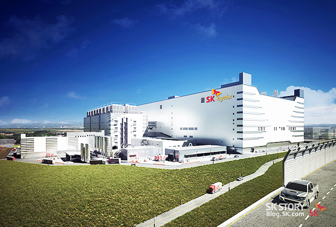
The new cluster will house four huge semiconductor fabrication plants, which will be located on a 4.15 million square-meter site, reports The Korea Herald. The four fabs will have a planned capacity of around 800,000 wafer starts per month (WSPM), which will make the site one of the world's biggest semiconductor production hubs. Keeping in mind that we are dealing with EUV fabs, it is not surprising that a huge 200,000-WSPM plant with EUV tools will cost SK Hynix north of $25 billion. The fab cluster will be located near Yongin, South Korea, 50 kilometers south of Seoul, according to Yonhap news agency that cites the Ministry of Trade, Industry and Energy.
The new fabs will be used to make various types of DRAM using SK Hynix's upcoming production technologies that will use extreme ultraviolet (EUV) lithography. And with a start date still years away, we're likely looking at a fab that will be used to manufacture DDR5, LPDDR5X, and other future types of DRAM.
SK Hynix reportedly plans to start construction of the first fab in the Yongin cluster in the fourth quarter of 2021. Given the expected size of the massive building and the amount of time needed to folly load it with production equipment, SK Hynix expects this first fab to be completed in 2025.
It is necessary to note that just several years ago SK Hynix and Samsung used to build fabs that could produce both DRAM and NAND flash memory – or at least be converted with a minimal amount of effort. This is not the case today as DRAM production now heavily relies on lithography equipment, whereas 3D NAND production uses loads of etching tools, which is why the fabs for different types of memory have to be equipped completely differently.
The fab cluster in Yongin will be SK Hynix's second major DRAM site in South Korea after the company's primary DRAM hub near Icheon that houses its M10, M14, and M16 fabs. The M16 fab was completed in February and will be used for DRAM production using SK Hynix's EUV-based 1a process technology starting the second half of 2021.